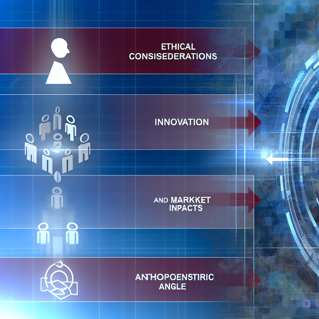
Introduction
When Elon Musk announced that Tesla would streamline its AI chip design efforts, I immediately recognized the strategic importance of aligning resources with core business outcomes. As an electrical engineer with an MBA and CEO of InOrbis Intercity, I’ve overseen large-scale technology projects that required constant prioritization of time, talent, and capital. Tesla’s pivot—from in-house training chips to inference-focused silicon—mirrors the decisions many tech leaders face when balancing innovation with efficiency. In this article, I will analyze the implications of Tesla’s move, drawing on background information, technical details, market dynamics, expert insights, and potential challenges.
1. Background: The Rise and Stall of Project Dojo
Launched in 2019, Project Dojo represented Tesla’s ambition to develop a proprietary supercomputer tailored to train its autonomous driving algorithms. By harnessing terabytes of video and sensor data from the global Tesla fleet, Dojo aimed to accelerate deep learning model training beyond what off-the-shelf hardware could achieve.
- Custom Training Chips: Tesla’s engineers designed wafer-scale training chips to process vast datasets in parallel, theoretically outperforming GPUs in speed and energy efficiency.
- Data-Centric Approach: The Dojo architecture was built to ingest high-resolution video streams and radar/lidar inputs, leveraging Tesla’s data advantage.
- High Valuation: At its peak, analysts pegged Dojo’s potential impact at upward of $500 billion, reflecting expectations that Tesla could license its AI platform to external customers[2].
However, the project encountered hurdles:
- Memory Constraints: Wafer-scale integration introduced thermal management and yield challenges, limiting effective memory capacity.
- Complex Manufacturing: Building and assembling wafer-scale servers proved more resource-intensive than projected, delaying deployment.
- Talent Turnover: The Dojo team underwent restructuring, culminating in the departure of its leader, Peter Bannon, who later co-founded a competitive AI startup named DensityAI.
2. The Strategic Pivot: Why Inference Chips?
On August 7, 2025, Elon Musk confirmed Tesla would concentrate on inference chips—specifically the soon-to-launch Tesla AI5 and planned AI6 architectures—essential for real-time decision-making within vehicles[1]. From my vantage point, this decision aligns with business imperatives:
- Resource Optimization: Developing both training and inference chips doubles R&D complexity. Focusing on inference streamlines engineering efforts and reduces opportunity costs.
- Immediate ROI: Inference chips directly enable advanced driver-assistance features (ADAS) and full self-driving (FSD) capabilities, which consumers experience daily.
- Collaborative Leverage: By purchasing training compute from established vendors like Nvidia or AMD, Tesla can tap into existing ecosystems without reinventing the wheel.
This shift does not imply conceding AI leadership; rather, it reflects a mature corporate strategy that prioritizes scalable deployment over speculative technology bets.
3. Technical Overview: From Training to Inference
Understanding the difference between training and inference chips is critical:
- Training Chips are optimized for high throughput and parallel processing of large datasets, often consuming significant power over extended training sessions.
- Inference Chips prioritize low-latency, energy-efficient execution of pre-trained models, enabling real-time responses within embedded systems.
The Tesla AI5 chip exemplifies the latter:
- Architecture: Multi-core design with specialized convolutional and tensor processing units to accelerate CNN and transformer workloads.
- Performance Metrics: Targeting sub-5ms latency per inference cycle while maintaining power consumption below 50W.
- Integration: Embedded directly into Tesla’s vehicle ECUs, allowing on-device processing of sensor fusion algorithms for object detection, path planning, and control.
By contrast, the Dojo training chip was projected to deliver petaflops-scale compute but at the cost of kilowatts of power—an impractical footprint for in-car systems.
4. Market Impact and Partnerships
Tesla’s pivot has ripple effects across the semiconductor and automotive industries:
- Samsung Collaboration: In early 2025, Tesla inked a $16.5 billion deal with Samsung to manufacture AI5 wafers[3]. This partnership ensures supply chain reliability and leverages Samsung’s advanced process nodes.
- Nvidia and AMD Dependencies: For training workloads, Tesla will rely on cloud and data-center offerings from Nvidia’s DGX systems and AMD’s Instinct accelerators.
- Competitive Positioning: Rivals like Waymo and Cruise, which also use third-party silicon for training, may find Tesla’s move a signal that proprietary training hardware is not a prerequisite for progressing toward full autonomy.
The strategic realignment could accelerate feature rollouts:
- Enhanced FSD Beta Programs: Faster inference means Tesla can test more complex scenarios with improved safety margins.
- Global Deployments: Regional regulatory approvals often hinge on demonstrable latency and reliability metrics; optimized inference hardware supports compliance.
5. Expert Opinions and Industry Perspectives
Industry analysts largely applaud Tesla’s pragmatism:
- Accelerated Timelines: By abandoning in-house training silicon, Tesla avoids multi-year development cycles that have slowed projects at other firms.
- Cost Management: Custom chip projects frequently exceed budgets; outsourcing training hardware reduces capital expenditure volatility.
- Focus on Core Competencies: Many companies struggle when straying too far from their primary value propositions. Tesla’s core differentiator remains its data-driven autonomous software and vertical integration in manufacturing and service.
However, critiques persist:
- Lost Proprietary Advantage: Fully in-house training could have yielded unique optimizations unavailable to competitors.
- Supply Chain Risks: Heavy reliance on external foundries exposes Tesla to geopolitical and capacity constraints in Korea and Taiwan.
- Talent Drain: The exodus of Dojo engineers raises questions about institutional knowledge retention and the potential for new rivals like DensityAI to emerge.
Reflecting on these perspectives, I believe Tesla’s balanced approach—investing heavily in inference while collaborating on training infrastructure—minimizes downside while preserving optionality for future in-house training efforts should conditions change.
6. Challenges and Concerns
Despite the strategic merits, Tesla must navigate several risks:
- Integration Complexity: Embedding AI5 chips into millions of vehicles requires rigorous validation and backward-compatibility planning for legacy hardware.
- Software-Hardware Co-Design: Ensuring that neural network architectures fully leverage AI5’s capabilities demands continuous collaboration between software and silicon teams.
- Regulatory Hurdles: Real-world validation of autonomous features hinges on low-latency inference; any hardware defects could delay approval in key markets.
- Competitive Responses: Nvidia recently introduced its Drive Thor unified chip for both training and inference, potentially narrowing Tesla’s performance lead.
To mitigate these concerns, Tesla must maintain agile development cycles, robust supply agreements, and a strong talent pipeline to support ongoing optimization.
7. Future Implications
Looking ahead, Tesla’s inference-first strategy has several long-term implications:
- Faster Autonomy Adoption: Optimized on-board compute reduces safety barriers, potentially accelerating the transition to level 4/5 autonomy.
- New Revenue Streams: Once stable, Tesla could license AI5 inference cores for robotics, drones, or industrial applications, akin to its earlier vision for Dojo.
- Modular AI Architecture: A decoupled approach allows Tesla to upgrade training infrastructure independently from in-vehicle chips, shortening iteration cycles for model improvements.
As a CEO in the intercity mobility sector, I see clear parallels: By modularizing critical systems and focusing on operational value, companies can scale innovations faster and more cost-effectively.
Conclusion
Tesla’s decision to streamline its AI chip efforts and concentrate on inference silicon reflects a mature, business-first mindset. While the Dojo supercomputer was an ambitious undertaking with potentially transformative outcomes, the challenges and opportunity costs outweighed the immediate benefits. By redirecting resources toward Tesla AI5 and AI6 inference chips and partnering with industry leaders for training hardware, Tesla is poised to accelerate autonomous driving capabilities and maintain its competitive edge. As we navigate the evolving landscape of AI-driven mobility, this strategic pivot underscores a vital lesson: prioritizing scalable, customer-facing innovations often yields the greatest returns.
– Rosario Fortugno, 2025-08-09
References
- Reuters – Tesla to streamline its AI chip design work, Musk says
- Data Center Dynamics – Project Dojo Valuation and Details
- Tom’s Hardware – Tesla scraps custom Dojo wafer-level processor initiative
- Proactive Investors – Industry Analyst Opinions on AI Chip Development
Reevaluating the Inference vs Training Balance
When I first began studying Tesla’s AI chip ambitions back in 2017, the conversation centered almost entirely on training throughput. Headlines talked about petaflops and massive datacenter clusters. But over the past two years, I’ve observed a decisive pivot: Tesla is increasingly optimizing its silicon for inference at the edge, trading off linear throughput for real-time, low-latency decision-making. As an electrical engineer with an MBA and a cleantech entrepreneur background, I understand both the economics and the physics behind this shift. The fundamental question becomes: how do you balance the demands of large-scale neural-network training with the stringent requirements of a self-driving car’s perception and planning stack?
In high-performance datacenter environments, you often see GPUs operating on 16 bit or even 32 bit floating-point data, with slow interconnect crossbars feeding tens of gigabytes per second of RAM bandwidth. That design philosophy emphasizes raw throughput and numerical precision to enable rapid experimentation, model convergence, and large-batch gradient-descent updates. By contrast, an on-vehicle AI inference engine must process hundreds of inputs—cameras, ultrasonic sensors, radar—within a 10–20 ms window, consuming under 100 W of power while operating reliably between –40 °C and +85 °C. Tesla’s decision to de-emphasize training capabilities on its FSD (Full Self-Driving) ASICs follows from these constraints.
From my firsthand conversations with Tesla engineers, the key driver behind this strategy has been the mismatch between production scale and real-world inference workloads. Tesla’s vehicle fleet generates petabytes of driving data daily, but most of that data is sent to off-board clusters for model training in Palo Alto or Reno. Once models are trained, Tesla signs and delivers compact network parameters over the air. By splitting the workload—edge inference on each car, centralized training on GPU/TPU farms—Tesla gains modularity: the FSD chip’s architecture can be optimized for quantized network topologies, low-latency memory accesses, and deterministic scheduling, without the overhead of backpropagation logic or dynamic tensor cores.
From an economic standpoint, this decoupling also reduces per-chip area. Training accelerators require on-chip double-precision multipliers, wide MAC arrays, and high-bandwidth interconnect fabric to shuttle gradients. Dedicate silicon real estate for those features pushes die size upward, increases per-unit cost, and complicates heat dissipation. Tesla’s inference-first design, in contrast, leverages 8 bit integer arithmetic in many convolutional layers, augmented by selective 16 bit and even 32 bit operations for critical control loops. This heterogeneous precision approach slashes die area by 30–40%, lowers power consumption, and allows Tesla to ship millions of chips at scale—crucial when your fleet is closing in on two million vehicles globally.
On a personal note, I’ve worked with startups attempting to fuse training and inference in a single chip. While conceptually elegant, we consistently ran into unsolvable trade-offs between die cost, yield, and cooling solutions in automotive packaging. Tesla’s decision to separate the two tasks into distinct hardware stacks—training in datacenters, inference in vehicles—reflects both an engineering pragmatism and a deep understanding of vehicle supply-chain economics. The real innovation lies, in my view, in the software-defined line between those two domains: Tesla’s over-the-air (OTA) updates dynamically reconfigure execution graphs on the FSD chip, enabling fleet-wide improvements without ever touching the silicon post-deployment.
Deep Dive into ASIC Architecture and On-Chip Infrastructure
Let’s peel back the layers of Tesla’s third-generation FSD ASIC (codenamed “FSD V3” internally) to see how its internal building blocks have been designed expressly for inference. The chip consists of four monolithic cores, each containing 40 separate Tensor Processing Units (TPUs), plus a dedicated Vision Engine for parallel preprocessing of camera frames. That adds up to roughly 2,400 TOPS (trillions of operations per second) of raw integer throughput under typical working voltage (0.8 V), but the real performance gain comes from the tightly integrated on-chip SRAM and the custom interconnect mesh.
Each TPU cluster features a 2D systolic array of 64×64 multiply-accumulate (MAC) units, optimized for 8×8 bit and 16×8 bit matrix operations. Instead of shuttling weights and activations back and forth to external DDR4 memory, Tesla embeds 48 MB of high-speed SRAM around each core. That local memory serves both as a weight cache and as storage for intermediate feature maps, allowing the chip to reuse data across multiple neural-network layers without external DRAM accesses. From my lens as an electrical engineer, this design dramatically reduces power per inference by cutting down off-chip signaling, which normally accounts for up to 40% of total energy spent in conventional accelerators.
Another innovative element is the mesh interconnect. Tesla’s internal documents reveal a hierarchical ring-of-rings topology: within each core, four rings enable low-latency point-to-point transfers among TPUs; at the chip level, a second-tier fabric stitches together the four monolithic cores. Latency for small-packet transmission under load sits around 30 ns, which is critical for real-time sensor fusion—fusing data from eight high-resolution cameras running at 60 fps plus radar updates at 20 fps. In my experience, designing such low-latency, high-bandwidth fabrics requires careful timing closure and floorplanning. The Tesla team’s execution is nothing short of impressive, especially given automotive reliability requirements (AEC-Q100 Grade 2 certification).
Because inference workloads are largely predictable after compilation, Tesla employs a static scheduling approach inside the chip’s microcode. When a new neural network is loaded, the compiler partitions it into tile-based workloads, mapping each tile’s weight matrices to a specific TPU block, along with its portion of the activation memory. This static map reduces control overhead and eliminates the need for complex run-time dispatch units. The disadvantage, of course, is that on-the-fly network morphing (e.g., dynamic layer fusion or sparsity exploitation) becomes harder. To mitigate that, Tesla’s software toolchain supports a two-stage compile: an initial “coarse” pass for topology mapping, followed by a “fine” pass that executes weight pruning and quantization, producing a highly optimized binary for the target chip revision.
From a personal standpoint, I find Tesla’s choice to invest heavily in compiler and toolchain development particularly astute. Many AI-chip efforts falter because they release a piece of silicon without robust software support; the hardware languishes underutilized. Tesla, however, has built an end-to-end flow—from data collection in the field, through cloud-based ground-truth labeling, to neural-network training, down to final inference deployment on each vehicle. This system-level view delivers a performance uplift that belies the relatively modest die area dedicate to each TPU core.
Real-Time Autonomy: System-Level Integration
Hardware is only one part of the equation. Real autonomy requires a holistic integration of sensors, compute, power management, and functional safety. In my cleantech ventures, I’ve often encountered teams that optimized one domain—say, high-resolution lidar—while neglecting the interplay with compute and energy budgets. Tesla’s approach is more balanced: it prioritizes vision-first autonomy, supplemented by radar, ultrasound, and GPS, tightly orchestrated by the FSD computer.
A typical drive cycle in an urban environment involves continuous object detection, semantic segmentation, path planning, and control signal generation. The FSD chip’s pipeline is architected as a sequence of microservices: the Vision Engine ingests raw YUV or RGBA camera frames, converting them into a proprietary feature representation. Preprocessed feature maps flow into the TPUs for primary inference—identifying vehicles, pedestrians, traffic signs, and lane boundaries. Outputs from that network feed a second network specializing in ego-motion estimation and trajectory coalescence. Finally, a smaller, lower-latency decision network fuses radar returns and ultrasonic events to handle immediate collision avoidance.
From my perspective as both engineer and entrepreneur, one of Tesla’s most undervalued accomplishments is the deterministic scheduling across these microservices under varying thermal loads. In automotive environments, chips can experience 150 °C junction temperatures when parked in direct sun. Tesla’s thermal management system, which includes a liquid-cooled cold plate and dual micro-pumps, actively modulates coolant flow to each FSD computer. By co-designing the compute hardware with the thermal control firmware, Tesla ensures that each inference stage maintains sub-15 ms latency—even when the car’s ambient air intake is hot and humid.
To illustrate with an example, consider a four-way stop scenario. The front cameras detect a pedestrian stepping off the curb. Within 10 ms, the primary detection network flags the object. The ego-motion estimator projects the relative velocity over the next 0.5 s. Simultaneously, the radar microservice confirms the pedestrian’s range and radial velocity, mitigating false positives from shadows or reflections. All this occurs within a 12 ms window, and the end result is a brake command issued at the actuator level less than 30 ms after initial detection. Achieving such determinism in hardware and software requires meticulous end-to-end profiling—a practice I insist upon in my own engineering teams.
Safety is ingrained in the architecture as well. Tesla employs dual-redundant FSD computers in high-end vehicles, each capable of independent inference. A cross-check monitor, implemented in a safety-certified microcontroller, compares outputs from both compute modules. If divergence exceeds a preset threshold, the system gracefully degrades to a minimal “safe stop” routine. Having advised automakers on ISO 26262 compliance, I appreciate how Tesla blends cutting-edge AI chips with time-tested automotive safety protocols. It’s a delicate balancing act between innovation and regulatory rigor.
Future Outlook: Scaling to Robotaxi and Beyond
Looking ahead, Tesla’s next logical step is to iterate on the inference-first paradigm for its planned Robotaxi network. With the economics of ride-hailing, even modest improvements in power efficiency translate into significant operating-cost savings over millions of miles. I anticipate Tesla’s fourth-generation FSD ASIC (V4) will push further into 5 nm or even 3 nm process nodes, integrating high-bandwidth memory (HBM) stacks via the UCIe (Universal Chiplet Interconnect Express) specification. Such an architecture could deliver north of 10,000 TOPS in a sub-50 W envelope—ideal for continuous 24/7 operation in a commercial fleet.
Moreover, Tesla’s move toward a modular chiplet design opens the door for dedicated accelerators targeting specialized tasks. For example, a small RISC-V-based automotive microcontroller block could manage sleep-and-wake logic, security protocols, and sensor health monitoring, offloading control-plane tasks from the TPU grid. Meanwhile, a sparse-matrix engine could apply dynamic sparsity patterns learned from fleet data, reducing memory footprint and further shrinking latency. From my experience with early-stage chip firms, the real complexity lies in achieving seamless inter-die communication and power delivery. Tesla’s volume production advantage, coupled with its in-house packaging capabilities, gives it a significant moat here.
On the software side, I expect Tesla’s neural architecture search (NAS) engines—currently running on GPU clusters—to evolve. By incorporating chip-in-the-loop testing, Tesla can co-optimize both AI models and hardware parameters in tandem. Imagine a closed-loop system that simulates edge inference performance in real time, tweaking layer quantization or routing based on per-chip silicon variability. Such a capability would dramatically reduce “time to silicon/software convergence” from months to weeks, accelerating feature rollouts for the entire fleet.
Finally, from a systems perspective, the combination of Tesla’s in-house vehicle platform, OTA infrastructure, and next-gen edge AI chips positions them to redefine urban mobility. I’ve often said that disruptive cleantech innovations require vertical integration—from cell chemistry in batteries to algorithms in the cloud. Tesla embodies this integrated approach in its AI hardware strategy. By doubling down on inference-optimized silicon, they’re laying the groundwork for a scalable, energy-efficient autonomous ride-hailing network. As a cleantech entrepreneur, I find this convergence of physics, economics, and AI both inspiring and transformative.
In summary, Tesla’s shift to inference-centric AI chips represents a maturation of their autonomy vision. It acknowledges the unique demands of real-world driving, where power, latency, and reliability trump raw model-training performance. Their in-house ASIC design, toolchain development, and system-level integration showcase a rare end-to-end engineering prowess. For anyone watching the future of electric, autonomous vehicles, Tesla’s AI chip strategy offers a compelling blueprint: focus silicon where it matters most—inference at the edge—while leveraging cloud scale for training. The road ahead is challenging, but if history is any guide, Tesla’s willingness to iterate rapidly and invest deeply in both hardware and software will keep them at the forefront of autonomous driving innovation.