Vertical Compute and imec have expanded their partnership to advance vertically integrated memory, an architecture that places dense memory directly above compute logic rather than beside it on a conventional chip. Announced on November 11, the program will use imec’s NanoIC pilot line to move the technology from validation work toward a 16nm manufacturing process.[1]
The development matters because AI hardware is increasingly constrained by the cost, energy use and latency of moving data between processors and memory. Stacking memory over logic will not eliminate that bottleneck, but it could substantially shorten the interconnects that move weights, activations and intermediate data. The important qualification is that this is a manufacturing-development step, not evidence of a qualified commercial product or high-volume deployment.
By the numbers
- 16nm: The process target identified for the manufacturing-development effort.
- November 11, 2026: Date imec announced the expanded partnership.
- Two active layers: High-density memory and compute logic are intended to be integrated vertically in the proposed architecture.

Why the memory-to-logic distance matters
Modern AI accelerators devote substantial silicon area, packaging complexity and power budget to feeding compute units with data. Arithmetic operations are highly parallel and increasingly efficient, but useful throughput depends on whether data can arrive at those units fast enough. When memory sits farther away, designers must use wider interfaces, larger on-chip caches, advanced packages and more aggressive power-management schemes to sustain bandwidth.
Vertical Compute’s premise is to address part of that problem physically. Instead of treating the memory array and compute logic as neighboring blocks connected across a chip or package, the company is pursuing memory fabricated directly above the logic layer. That can reduce wiring length and potentially increase connection density between memory and compute.
The appeal is especially clear for AI inference and data-intensive workloads, where repeatedly moving model parameters between memory and processing elements can consume more energy than the associated arithmetic. A shorter path can reduce capacitive switching energy and improve bandwidth per unit area. It may also allow designers to devote less die area to long-distance routing.
Those benefits are architectural possibilities, not performance results from the new announcement. Actual gains will depend on the memory technology, layer-to-layer interconnect density, thermal behavior, yield, access latency, software mapping and the application’s data-reuse pattern. Some AI workloads are limited by memory bandwidth; others are constrained by compute, external memory capacity or communication among accelerator chips.
What moving into imec’s NanoIC pilot line changes
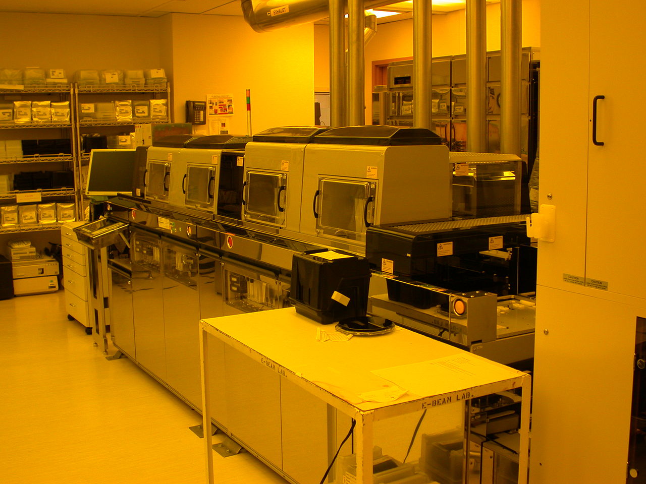
imec’s NanoIC pilot line is central to the significance of the partnership expansion. A design can be compelling in simulations or in isolated test structures while remaining difficult to manufacture consistently. Pilot-line work brings the technology into a setting intended to evaluate process integration: how sequentially built layers interact, whether overlay and alignment are sufficiently precise, how contacts are formed, and whether the resulting devices can be characterized with a manufacturing-oriented discipline.
For vertically integrated memory, the challenge is not simply putting one layer on another. The logic beneath the memory must survive the added processing steps. Thermal budgets must be controlled so that later fabrication does not degrade the already-built devices and interconnects. Wafer handling, contamination control, planarity, defect inspection and electrical testing all become more consequential when defects in either layer can affect the finished stack.
imec said the collaboration is intended to accelerate commercial manufacturing of Vertical Compute’s technology and move it toward a 16nm process.[1] That phrasing is meaningful because it shifts the work beyond a general research relationship and toward a defined process-development objective. A 16nm target is also more relevant to potential production economics than an experimental demonstration at a laboratory-only node, even though it is not equivalent to a product launch.
The announcement does not establish a production foundry, a customer program, a tape-out date, production yield, reliability qualification or cost per bit. It also does not provide comparative measurements for energy, bandwidth, latency or density. Those are the evidence points that customers and manufacturing partners will need before judging whether vertical integration can compete with conventional memory hierarchies and advanced packaging approaches.
Key organizations and the manufacturing challenge
Vertical Compute is the technology developer seeking to commercialize the vertically integrated memory architecture. imec, the Belgium-based semiconductor research and innovation organization, provides process-development infrastructure and expertise through its NanoIC pilot line. Their expanded relationship joins an architectural proposition with a fabrication environment designed to test whether the proposition can be translated into repeatable process modules.[1]
The division of labor reflects a broader semiconductor reality. Startups can develop specialized device concepts and intellectual property, but commercialization depends on process integration, equipment compatibility, metrology, design rules and access to a manufacturing ecosystem. Pilot-line validation can expose limitations that are invisible in a device-level prototype: unacceptable variability, difficult inspection, low tolerance for defects or process steps that are too expensive to scale.
Industry engineers generally view this transition as the point at which claims become more testable. The relevant question is no longer only whether a vertical stack can function electrically. It is whether it can deliver a useful combination of yield, reliability, thermal performance, density and cost. In memory, where margins and volumes are tightly linked to manufacturing efficiency, an elegant architecture with poor yield will struggle to reach the market.
Where this fits in the AI hardware market
The effort arrives as AI-system designers search for ways to relieve the so-called memory wall. High-bandwidth memory, chiplets, advanced 2.5D packages and three-dimensional stacking are all attempts to increase data movement efficiency without relying solely on faster logic transistors. Vertical Compute’s approach belongs to that wider push, but differs in emphasizing a close, vertically integrated relationship between high-density memory and compute logic.
If successful, such integration could be useful where a compact accelerator needs high local bandwidth and lower data-movement energy. Edge systems, inference accelerators and specialized data-center silicon are plausible categories, although imec’s announcement does not identify a first product market. The architecture could also influence system design by shifting more memory closer to compute, potentially reducing pressure on some external interfaces.
There are trade-offs. More tightly coupled layers can complicate heat removal, test and repair. Memory and logic often favor different manufacturing processes, and a process that is optimal for one may impose compromises on the other. Capacity also matters: a tightly integrated memory tier may be extremely fast but still insufficient for larger AI models, leaving a system dependent on off-chip memory and interconnects.
Competition will not come only from other vertical-memory concepts. Established suppliers are improving high-bandwidth memory stacks, packaging vendors are expanding interposer and hybrid-bonding capabilities, and AI-chip designers are adding larger SRAM caches and more sophisticated dataflow architectures. Vertical Compute will therefore need to demonstrate not merely that its stack works, but that it offers a clear system-level advantage over alternatives that are already entering products.
Milestones that would turn a process target into market evidence
The next indicators will be technical and commercial. On the technical side, observers should look for disclosed test-chip results, memory density, interconnect pitch, bandwidth, latency, energy per transferred bit, thermal data and reliability results. On the manufacturing side, the critical disclosures would include wafer-scale yield, defect-management methods, compatibility with standard fabrication equipment and a credible path from pilot-line processing to a manufacturing partner.
Product evidence will matter most. A named customer, a packaged demonstrator, a system benchmark against a conventional memory-plus-logic design, or an announced path to qualification would carry more weight than another architecture diagram. The 16nm objective provides a concrete point around which those tests can be organized, but it is an intermediate engineering target rather than proof that the technology is ready for volume production.
For AI hardware, the larger implication is that future efficiency gains may increasingly come from physical data locality as much as from new compute architectures. The industry has already learned that adding more arithmetic units does little when memory cannot keep them busy. Vertical integration is one possible answer; imec’s pilot-line work will help determine whether this particular answer can be manufactured economically.
Editor’s Take
I see this as a credible and useful shift from a promising chip concept into the harder part of semiconductor development: proving that a stack can be built repeatedly, not just demonstrated once. Putting dense memory directly above logic attacks a real source of AI cost—data movement—and the 16nm process target gives the collaboration a more concrete commercial frame than a research-only announcement.
The hype would outrun the facts if this were treated as a new memory product today. It is not. I would watch for yield data, thermal results, reliability qualification and a benchmark that measures whole-system energy rather than an isolated interconnect. If those results are strong, the technology could become valuable precisely because it improves AI hardware without requiring developers to wait for a radically different model or software stack.